The SIS3600 is the latch firmware implementation on the base of the SIS360x/38xx base board. The module is designed as a multi event latch with a default FIFO size of 32 K events, 128 K events can be implemented as stuffing option. The user can select between strobed and coincidence mode via a bit of the control register, a fast clear window can be programmed via a register and activated by a key address. The module is available with ECL, TTL and NIM input level, ECL and TTL units are available with flat cable connectors, TTL and NIM units with LEMO connectors. The board can also be used as a VME input FIFO for ECL, TTL or NIM data streams, the maximum speed reaches 20 MB/s (i.e. 200 ns/ per 32-bit word).
The unit looks exactly like the SIS3800 flat or SIS3800 LEMO units
32-bit
ECL, NIM, TTL or LVDS input levels
LEMO (NIM, TTL) or flat cable (ECL, LVDS) connectors
32 K (128 K optional) events
FIFO structure
Fast OR output
Fast clear capability
strobed and coincidence mode
VME Access/user LED
A16/A24/A32 D16/D32
CBLT32 in Firmware Version 2
VME64x Connectors
VME64x Side Shielding
The SIS3600 can be operated in strobed and in coincidence mode. The mode of operation is selected through the control register. It will depend on the given application, which mode is more appropriate.
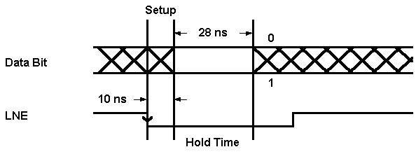
The strobed mode of operation is suited for the acquisition of data streams or the readout of trigger patterns to give two examples. In strobed mode the input level (0/1) of the 32 inputs is latched with the leading edge of the so called LNE (load next event) signal, which can be regarded as write strobe in the data stream application case. The datum has to be stable after the setup time for the duration of the hold time.
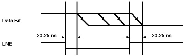
The coincidence mode of operation is suited for applications, in which it is of interest, whether a hit occured within a time window or not. The time window is defined by the LNE (load next event) signal. Inputs with a level transition from 0 to 1 will be latched as 1, all other conditions (constant 0/constant 1/transition 1 to 0) will result in a latched 0. For safe recognition the of bit change the setup and hold timing will have to be taken into account as sketched below.
If fast clear mode is enabled by access to the corresponding key address, events with an external fast clear pulse within the fast clear window (FCW) will be discarded. The fast clear window can be programmed via the 8-bit deep fast clear window register in steps of 100 ns, i.e. the maximum duration of the fast clear window is some 25 µs. The CIP (copy in progress) output will be active for the duration of the FCW.