VME Setup with 16 SIS3300 modules and SIS3100 at the South Pole
(Photograph courtesy of Amanda collaboration)

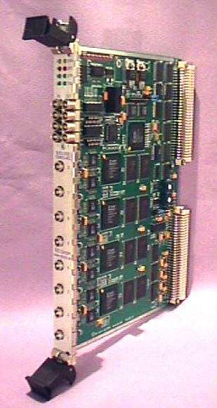
The SIS3300 is an 8 channel 6U VME digitizer/transient recorder with a sampling rate of up to 105 MHz (for the individual channel) and 12-bit resolution. The board has a width of one VME slot (4TE). The boards multi event and dual memory bank functionality make the card the choice for many demanding digitizer applications.
The SIS3301 65/80/105 MHz 14-bit FADC is the second member of this board family.

|
VME Setup with 16 SIS3300 modules and SIS3100 at the South Pole (Photograph courtesy of Amanda collaboration) |
Szifi Calorimeter readout
NaI crystal readout
Gamma spectroscopy
Strip detector readout
Digitization of serialized data
Beam diagnostics
Single width 6U VME card
8 channels (stripped 4 channel version available)
105 MHz per channel (1 MHz - 105 MHz)
>80 MHz bandwidth
Internal/External clock
2 banks x 128K samples/channel memory
Multi event mode
Pre/Post trigger capability
Trigger or output (8 individual thresholds)
A32/D32/BLT32/MBLT64/2eVME
In field JTAG firmware upgrade capability
Trapezoidal FIR filter option (firmware major revision 0x11) see below
Power consumption: +5V 6A (sampling @ 100 MHz), +12 V 50 mA, -12 V 50 mA
| Control In/Outputs | |
| Inputs | Outputs |
| Clock In | Clock Out |
| Start | Busy |
| Stop | Trigger |
| User in | User out |
Control In/Outputs are available with NIM or TTL levels
|
LED's |
|
| A (Access) | Sam (Sampling) |
| P (Power) | SRT (Start) |
| R (Ready) | STP (Stop) |
| U (User) | TRG (Trigger) |
| Input Options |
| LEMO00 connectors, 0 ... -/+1 V 50 Ohm inputs |
| LEMO00 connectors, 0 ... -/+5 V 50 Ohm inputs |
| LEMO00 connectors, 0 ... -/+8 V 75 Ohm inputs |
| LEMO00 connectors, +2.5 ... -2.5 V 50 Ohm inputs |
| other range and impedance options on request |
| refer to SIS3301 for differential input options |
| Memory Options |
| All units are stuffed with two memory banks (2 x 128 KSamples/channel) to allow for readout in parallel to acquisition/sampling |

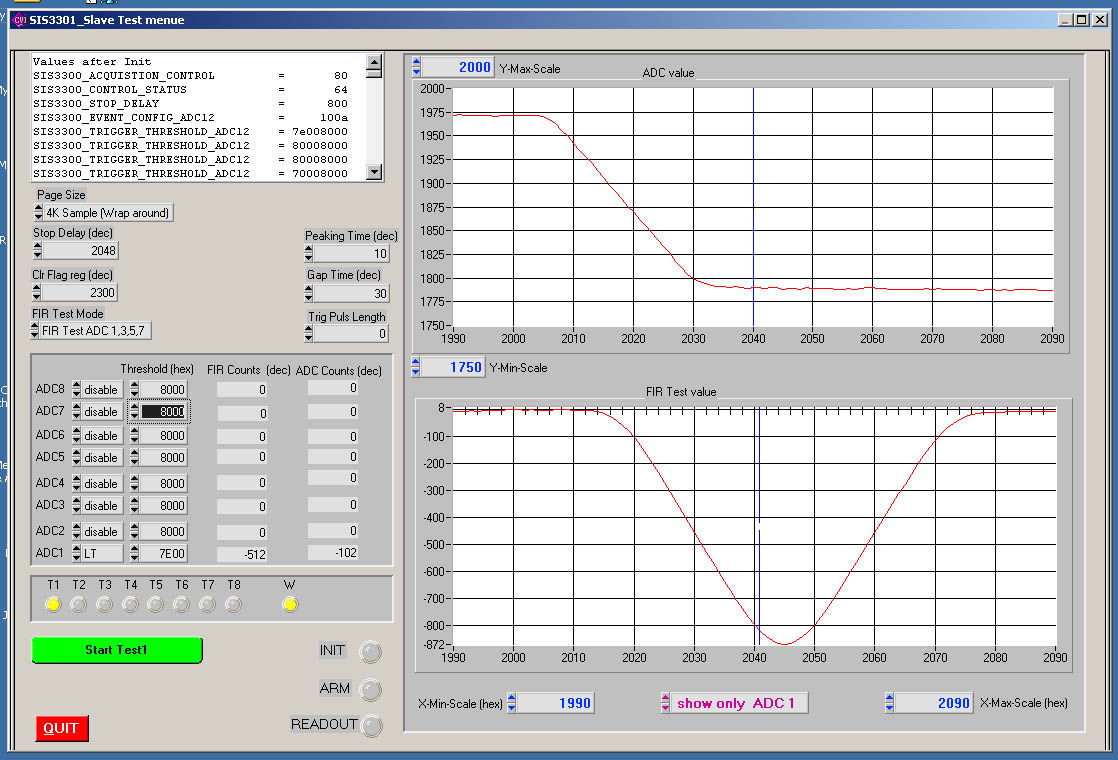
A trapezoidal filter was implemented for DC/offset independent trigger generation. The screen shot below shows the input on ADC channel 1 and the corresponding FIR filtered data (which can be stored to ADC memory in test mode also).